Abstract—Addition, a fundamental operator in modern computational systems, has a multitude of highly optimized implementations. In general purpose systems, the width has grown to 128 bits, putting pressure on designers to use sophisticated carry lookahead or tree adders to maintain throughput while sacrificing area and energy. However, the typical workload mostly exercises the lower 10 to 15 bits. This leaves many devices on and unused during normal operation, reducing the overall performance. We hypothesize that bit- or digit-serial implementations for arbitrary-length streams represent an opportunity to decrease the overall energy usage while increasing the throughput/area efficiency of the system and verify this hypothesis by constructing an asynchronous digit-serial adder for comparison against its bit-parallel counterparts.
Keywords—addition, arithmetic, asynchronous, quasi-delay insensitive, qdi, bundled-data, bd
Introduction
Arithmetic plays a central role in computation. Of all assembly instructions executed in the SPEC2006 benchmarks, 47% are arithmetic operations, 26% are integer arithmetic, and 10% are integer adds. Yet, interest in this subject declined in the late 1990's suggesting that further research has been providing diminishing returns [10].
The majority of high performance processors since the 1970s have been bit-parallel architectures with ever increasing bitwidths. While algorithmic requirements have been the primary factor driving the datapath to 32 bits, large dynamic memory requirements have recently pushed the datapath towards 64 bits and beyond. [9]
This has encouraged significant research toward a varied array of bit-parallel arithmetic circuitry [13]. The Ripple-Carry Adder is simple and energy efficient but ultimately slow, producing a result in a worst case linear time. The Manchester Carry Chain improves upon this structure using pass transistor logic along the carry chain [23]. Sacrificing area and energy for latency and throughput [15][16], there is a large class of carry-lookahead adders that produce a result in worst case logarithmic time [18][19][20][21][22]. Finally, there are hybrid adders that mix multiple strategies: tying four bit Machester Carry Chains together using Carry Lookahead techniques [25][26].
Recently, the power wall has limited device utilization and enforced a strict ceiling on clock frequency [11]. This combined with a surge of interest in highly parallel applications and AI, as indicated by a distinct change in focus between Spec2000 [7] and Spec2006 [8], has pushed researchers and architects to focus on specialized parallel cores, leading to a resurgence of interest in Coarse Grained Reconfigurable Arrays (CGRA).
CGRAs are effectively Field Programmable Gate Arrays (FPGA) with more complex computational blocks. They seek to maximize parallel throughput by taking advantage of spatial parallelism. The amount of spatial parallelism an architecture can support is determined by the number of function blocks that can fit within a given area budget. Therefore, architects have been exploring bit-serial arithmetic as a means of maximizing throughput per transistor. [34][38][36][37]
Since most CGRA architectures are clocked, they need the output of a function block to have predictable timing to keep the problem of mapping the design to the architecture tractable. This means that everyone ultimately uses the same topology for bit-serial arithmetic. For addition, an adder has its carry out fed back to its carry in through a multiplexer and a flip flop. Then, the multiplexer is given a control signal to determine whether to reset the flop. [30][29][31][33][28] Though one approach goes a little further to add overflow detection [32], the control ultimately remains rigid and system-wide, supporting only fixed-length operand streams.
While continually more energy has been put into resolving wider arithmetic, Fig. 1 shows that the average bitwidth of the algorithmic work has remained relatively constant at 12 bits and the bitwidth of the memory management work remains predictable at the full width of the memory bus, or 48 bits [5]. Because these architectures only support fixed-length streams, they miss most of the energy and throughput benefits attainable through serial arithmetic. While a fixed-length adder is more suitable for the memory management work, a length-adaptive architecture targeting the algorithmic work could support arbitrarily long streams while achieving average throughput and energy metrics similar to a 12-bit fixed-length architecture When applied to the algorithmic work.
We present control circuitry for length-adaptive addition and stream compression in self contained modules with their own control flow as inspired by BitSNAP, an adaptive bit-serial asynchronous microprocessor [35]. While BitSNAP's control and datapath were both implemented with Quasi Delay-Insensitive (QDI) design, we integrated a Bundled Data (BD) datapath with the QDI control. QDI's propensity toward complex control patterns and BD's propensity toward efficient datapath logic allow us to exploit the strengths of both synchronous and asynchronous design.
Section 2 describes our general design methodology. Section 3 describes length-adaptive addition. Section 4 and Section 5 describe full stream and single digit compression respectively. In Section 6, we show that our implementation is superior on average for both energy per operation and throughput per transistor to parallel ripple and lookahead adders. We also show that the benefits of length-adaptivity far outweigh its overhead and that the use of QDI design in the control leads to the most efficient approach. Finally, the Appendix gives an overview of the program and circuit notation used in this paper.
Integrated QDI/BD
QDI asynchronous circuits use additional circuitry that acknowledges each signal transition, preventing others until the resulting computation as been completed and the value is no longer necessary. These extra acknowledgement requirements make QDI circuits very robust to variable gate delays and allow architects to be meticulous about energy expenditure. However, they also introduce significant overhead when communicating the control behavior to the datapath and visa versa which is only exacerbated in wider datapaths.
Asynchronous micropipelines are a common way to take advantage of QDI's propensity towards complex control behavior by bundling a latched datapath with a QDI control. However, the QDI control tends to be very simple, the datapath tends to be wide, and a strict separation is maintained between the two. This paper explores a scenario in which complex control behavior is highly dependent upon some of the input data from a narrow datapath. In this scenario, it is more performant to integrate that data into the QDI control.
Ultimately, tying a bundled datapath to a non-trivial QDI control creates a few complexities. With a typical BD design, there is only one request. This makes the request optimal for the delay line and the clock signal to the latches in the datapath. However, because our control will have to deal with non-trivial QDI data encodings, there will be more than one request rail. This makes it more expensive to place delay lines and difficult to use as a clock signal.
There are three common topologies for designing handshake circuits: Weak Conditioned Half Buffer (WCHB), Pre-Charge Half Buffer (PCHB), and Pre-Charge Full Buffer (PCFB) [12]. If the control processes are PCHB or PCFB templates, then there is an internal cycle on which the delay line can be placed. However, if they are WCHB templates, then we are left with little choice but the request lines. If the QDI control requires a result from the datapath, then the input requests should be delayed until that result has been computed. Otherwise, they should be delayed until all of the input data has resolved and is ready to be latched. This means that different request lines can have different delay depending upon their dependencies with the datapath. Alternatively, extra logic can be used to generate and use a validity signal from the request lines. However, this strategy tends to require much longer transistor stacks in the forward drivers of the receiving process.
For clock signal generation and subsequent latches, the acknowledgement makes a good alternative to the request rails. While we lose the ability to count the necessary amplifier toward the delay line, we still have a clean one-wire signal with the right timing. Before any requests have been acknowledged, the latches should be open and ready to receive data. Upon acknowledgement, the latches should close so that the input data may be reset alongside the input requests.
Then, there is the final problem of making the control and the datapath interact. Any input signals from the QDI control to the datapath must be set up and stay stable such that the datapath has time to finish by the time the output enable is lowered, closing the output latches. The easiest way to handle this is with internal state in the control, setting its value on the downgoing transition of the output channel the iteration before.
Any output signals from the datapath to the control must be covered by the delay lines on the input request and remain independent from any signals communicated from the QDI control. This is because a change in the value of the internal state in the control could cause a change in the output signal from the datapath and therefore an instability in the QDI control. If there is a dependency, then the output signal from the datapath needs to be latched by the same signals that latch the internal state driving the input signals from the control.
Subsequently, we apply these ideas to design a new length-adaptive adder architecture that significantly outperforms existing designs in the literature.
Adaptive Adder
The fundamental algorithm for LSB first serial addition is fairly simple.
We assume that the two input streams are aligned such that the first token in
each stream represents the same digit-place. Then, digits arrive on the input
channels A and B in the same order that the carry
chain is propagated. So, they are added with the carry from the previous
iteration, ci, to produce the sum on the output channel
S and a new carry for the next iteration, co. The CHP
below describes the algorithm. ∗[ code ] is an infinite
loop and [ exp → code ▯ exp → code ] is an if
statement. See the Appendix for more details.
ci:=0;
∗[s  := (Ad + Bd + ci) % pow(2, N);
  co := (Ad + Bd + ci) / pow(2, N);
  S!s;
  A?,B?;
  ci:=co;
 ]
However, a real implementation must support finite length streams. So, we
add an extra bit to each token called cap
, which is only true for the
last token in the stream. To operate on two streams of differing lengths, we'll
sign extend the shorter stream by skipping the acknowledgement of its cap
token, repeating it until the cap token of the longer stream. Then, we
acknowledge both and continue to the next operation. Because streams can extend
to an arbitrary length, they can represent arbitrarily large numbers with a
fixed precision.
For addition, finite-length streams also introduce overflow conditions. When
both inputs are cap tokens, then two's complement dictates that their values
repeat. So the output values must also repeat. However, if co ≠
ci, then the next sum token will be different from the current one.
Extending the input streams by one more token on an overflow condition
guarantees that the co = ci on the next iteration and that
consecutive sum bits will all be the same. Then, we can reset ci
and complete the output stream by forwarding a cap token.
∗[s  := (Ad + Bd + ci) % pow(2, N);
  co := (Ad + Bd + ci) / pow(2, N);
  [ !Ac ∨ !Bc          → S!(s,0); co:=ci;
	        [ !Ac → A? ▯ else → skip ],
	        [ !Bc → B? ▯ else → skip ]
  ▯  Ac ∧ Bc ∧ co≠ci → S!(s,0); co:=ci
  ▯  Ac ∧ Bc ∧ co=ci → S!(s,1); ci:=0; A?,B?
  ]
 ]
Our implementation will start with the sign extension logic. This has four
cases defined by the intersection of Ac and Bc that
need to be implemented. In the first case, neither inputs are cap tokens. In
the second only A and in the third only B has a cap
token. Finally both inputs have cap tokens in the fourth case. Unfortunately,
none of these cases line up in the forward driver or acknowledgement logic. In
the forward drivers cases 0, 1, and 2 drive Sc0 and case 3 drives
Sc1. In the acknowledgement logic, A is only
acknowledged for cases 0, 2, and 3, and B for cases 0, 1, and 3.
This means that a typical QDI implementation of the control will likely be
incompatible with any other logic, forcing it to have its own pipeline
stage.
To avoid this problem, we can take advantage of the BD circuitry. We start
by using SR latches to store a static version of the input request. These are
placed before the delay lines on the input request to give them time to
stabilize before the QDI circuitry starts to operate. Each production
rule listed is the logical expression for a pull-up expr → var↾
or pull-down expr → var⇂ network in the circuit. Transistors in
series are represented by A ∧ B and in parallel by A ∨ B.
PMOS transistors are enabled when the gate voltage is low, signified
by ¬A. For example, the first production rule listed below
describes the pull-down network of the NOR gate driving
Ax1. To help understand this notation, we've rendered the
production rules for this process in Fig. 3 as a
transistor diagram. See the Appendix for more details.
Ax0 ∨ Ac0 → Ax1⇂
Ax1 ∨ Ac1 → Ax0⇂
¬Ax0 ∧ ¬Ac0 → Ax1↾
¬Ax1 ∧ ¬Ac1 → Ax0↾

Bx0 ∨ Bc0 → Bx1⇂
Bx1 ∨ Bc1 → Bx0⇂
¬Bx0 ∧ ¬Bc0 → Bx1↾
¬Bx1 ∧ ¬Bc1 → Bx0↾
Then, we combine the input requests before the delay lines. This reduces the
number of delay lines we need by two and has zero overhead with respect to the
rest of the control. After delaying AB, we are set up to implement
whatever control we want using AB as its input.
(Ac0 ∧ (Bc0 ∨ Bc1) ∨ Ac1 ∧ Bc0) → AB0↾
Ac1 ∧ Bc1 → AB1↾

¬Ac0 ∧ ¬Bc0 → AB0⇂
¬Ac1 ∧ ¬Bc1 → AB1⇂
Then, we need the comparison logic for Ci and Co.
To reduce the overall gate area, we use a pass transistor XOR to determine
whether Ci and Co are different. Because this XOR
will be used in the QDI handshake, the output of this XOR must remain high as
Ci is transitioning between values through its neutral state,
(1,1). This means that the usual pass transistor XOR is not
sufficient. However, we can use the fact that Co remains stable
through the QDI handshake and both Ci and Co are one
hot encodings.
passp(Cod1, Cid1, Dd1)
passn(Cod1, Cid0, Dd1)
passp(Cod0, Cid0, Dd1)
passn(Cod0, Cid1, Dd1)
Dd1 → Dd0⇂
¬Dd1 → Dd0↾
With the above setup, we can now implement the main cycle starting with the
forward drivers. Luckily, it can be drastically simplified by a few key
observations. First regarding the acknowledgement signals Ae and
Be, if AB is not a cap, then a non-cap token is
output on S, A is acknowledged if it's not a cap, and
B is acknowledged if it's not a cap. However, if AB is
a cap token, then there are two conditions. The overflow condition when
Co ≠ Ci also outputs a non-cap token on the output. It
acknowledges neither A nor B, and luckily both
A and B are cap tokens. So the acknowledgement is
automatically implemented by the same logic that handles the case in which
AB isn't a cap. The final case in which Co = Ci
outputs a cap token on S and so must be handled as a separate set
of logic anyways.
Second, on an overflow condition, both A and B are
cap tokens but Co ≠ Ci. This means that the inputs aren't
acknowledged, the next operation doesn't pass through the delay lines, and the
bundled-data timing assumption breaks.
However, because cap tokens must be all ones or all zeros, we know that if
Co is not equal to Ci, then the data on
A and B must be equal. If they weren't, then the
resulting addition would be all ones and the value on Ci would be
faithfully propagated to Co making them equal.
If A and B are all zeros, then Co is
guaranteed to be 0 meaning Ci must be 1.
In this case, only the least significant bit of the datapath changes. If
A and B are all ones, then Co is
guaranteed to be 1 and Ci must be 0. In
this case no bits are changed in the datapath. This means that the max delay
required by the datapath in this case is constant at one bit in the carry
chain, which is far less than the natural cycle time of the control process.
This allows us to implement extremely simple forward driver and acknowledgement
logic.
Se ∧ (ABd0 ∨ ABd1 ∧ Dd1)  → Sd0↾
Se ∧ ABd1 ∧ Dd0 → Sd1↾

Sd0 ∧ Ax0 ∨ Sd1 → Ae⇂
Sd0 ∧ Bx0 ∨ Sd1 → Be⇂
Third, if Co ≠ Ci, then setting Ci = Co won't
cause any transition on Co. The only time Co is
dependent upon the value of Ci is when all of the bits in the
adder propagate the carry. However, in that case Co is guaranteed
to be equal to Ci. This means that the value of Ci
can be both an input to the datapath and set by an output from the datapath
without any extra control circuitry.
¬Cid0 ∨ ¬Se ∧         ¬_Sd0 ∧ ¬Cod0  → Cid1↾
¬Cid1 ∨ ¬Se ∧ (¬_Sd1 ∨ ¬_Sd0 ∧ ¬Cod1) → Cid0↾
Cid0 ∧ (Se ∨        _Sd0 ∨ Cod0)  → Cid1⇂
Cid1 ∧ (Se ∨ _Sd1 ∧ (_Sd0 ∨ Cod1)) → Cid0⇂
Fourth, on the reset phase we check to make sure the next Ci has
the correct value before resetting the forward drivers and the acknowledgement.
Luckily, the overflow case doesn't acknowledge ABd1, so resetting
Sd0 only has to make sure ABd0 is acknowledged and
Ci = Co as evaluated by D.
¬Se ∧ ¬ABd0 ∧ ¬Dd1 → Sd0⇂
¬Se ∧ ¬ABd1 ∧ ¬Cid1 → Sd1⇂

(¬Sd0 ∨ ¬Ax0) ∧ ¬Sd1 → Ae↾
(¬Sd0 ∨ ¬Bx0) ∧ ¬Sd1 → Be↾
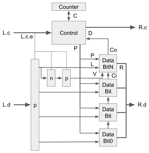
For the datapath shown in Fig. 2, we latch the input data
for A and B and clock the latches using
Ae and Be respectively. This along with the
Ci is fed into a Manchester Carry Chain which drives the output
data, Sd, and the carry-out, Co.
Compress Full
Suppose that our bundled-data adder has a datapath width of
N=4 bits. The resulting sum of 127, with an encoding of
0000 0111 1111, and -128, with an encoding of 1111 1000
0000, is -1, encoded with three tokens 1111 1111 1111.
However, encoding -1 requires only one.
So we compress the stream encoding by storing up each carry chain until we know if it contains the cap token. If yes, we only forward the cap. If no, we forward the whole carry chain and start again. However, a token may only be dropped if it is equal to the cap, meaning it must be all ones or all zeros. Tokens that aren't can bypass this carry chain logic.
The implementation requires two internal variables: v
represents the value of the bits in the carry chain using one bit, and
n counts the number of tokens in the carry chain that are
currently held. For clarity, the ext() function implements
sign-extension, the msb() function selects the most significant
bit in the token, and the chain() function returns true if a
token is all ones or all zeros.
v := 0, n := 0;
∗[∗[ Ld≠ext(v) ∧ n>0 → R!(ext(v),0); n := n-1 ];
  v := msb(Ld);
  [ !chain(Ld)        → R!(Ld,0)
  ▯  chain(Ld) ∧ Lc=0 → n := n+1
  ▯                Lc=1 → n := 0, R!(ext(v),1)
  ]; L?
 ]
Upon receiving a token, we first check if it's part of the stored carry
chain. If not, we know that carry chain doesn't contain the cap token. So, we
loop over n, draining the stored carry chain to the output.
Then, we start accumulating the next chain. So we set v to the
last bit in the input token and check if the input token is all ones or all
zeros. If neither, we forward it, bypassing the carry chain logic. Otherwise,
we increment n. If the input token is part of the carry chain
and is the cap token, then we clear the counter and forward the cap token.
Flattening this behavior leaves us with four basic conditions. Condition 1 implements the loop, decrementing when the input is not part of the carry chain. Condition 2 implements the bypass case when the input isn't part of any carry chain. Condition 3 implements the carry chain accumulation case that consumes inputs and increments the counter. Finally, condition 4 implements the cap condition in which the counter is cleared and the cap token is forwarded.
v := 0, n := 0;
∗[[  Ld≠ext(v) ∧ n≠0 → n := n-1, R!(ext(v),0)
  ▯ !chain(Ld) ∧ n=0 → v := msb(Ld); R!(Ld,0); L?
  ▯ Lc=0 ∧ (Ld=ext(v) ∨ n=0) →
                      n := n+1, v := msb(Ld); L?
  ▯ Lc=1 ∧  Ld=ext(v) → n := 0, R!(ext(v),1); L?
 ]]
This design exposes complex communication patterns between the control and datapath. While the acknowledgement requirements introduced by these patterns make a QDI-only implementation inefficient, a bundled data design saves us from most of these requirements. Ultimately, making intelligent choices about what is implemented in the datapath will make all the difference in creating a simple and efficient design.
The n and its associated increment, decrement, and clear
actions are implemented efficiently by the idczn counter from [4]. This provides a counter-flow interface that maps well
to the control's behavior.
We copy the MSB of Ld into v in every condition
that L is acknowledged except for the last. However, in the last
condition when the input is a cap token, the next value of v
doesn't matter because the associated clear guarantees that n
is 0. So our implementation can set v every time we
acknowledge L. This allows us to implement v as a
flip-flop in the datapath, making it accessable to the comparison operation
between Ld and ext(v), and its assignment to the
MSB of Ld.
The timing assumptions introduced by the bundled data design flow pose
new challenges in the design of the compression unit. In particular, the condition
that doesn't acknowledge L skips the delay lines and forces us
to consider other methods of implementing the timing assumption. In the case of
the bundled data adder, this just meant taking a hard look at the set of
resulting timings to prove to ourselves the delay line was unnecessary in the
first place.
For the control, we'll start by implementing the four forward driving cases.
The logic for these drivers uses three input data. Cz and
Cn implement a one of two encoding that signals whether the
counter is zero or not. Lc0 and Lc1 implement a one
of two encoding with the input request specifying whether this token is a cap
token, and D is a one of three encoding. Dd0 signals
that Ld=ext(v), Dd1 signals
Ld=ext(¬v), and Dd2 signals
!chain(Ld). D comes from the datapath and is
assumed to be stable by the time we receive a request on Lc0 or
Lc1.
The output signals are named by their interaction with the counter.
Cd decrements the counter, Cs has no action,
Ci increments the counter, and Cc clears it.
Rc0 is calculated from the internal nodes of the c-element
driving Cd and Cs, and Rc1 lines up
perfectly with Cc. Finally, all of the output requests except
Cd acknowledge the input.
Re ∧  Cn ∧ (Dd1 ∨ Dd2)      ∧ (Lc0 ∨ Lc1) → Cd↾
Re ∧  Cz ∧  Dd2                   ∧ Lc0 → Cs↾
     (Cz ∧ (Dd0 ∨ Dd1) ∨ Cn ∧ Dd0) ∧ Lc0 → Ci↾
Re ∧ (Cz ∧ (Dd0 ∨ Dd1) ∨ Cn ∧ Dd0) ∧ Lc1 → Cc↾

¬_Cd ∨ ¬_Cs → Rc0↾
Rc1 = Cc

Ci ∨ Cc ∨ Cs → Le⇂
This yields a fairly clean WCHB implementation, and the reset behavior is as expected.
¬Re ∧       ¬Cn        → Cd⇂
¬Re ∧             ¬Ld0 → Cs⇂
      ¬Cz ∧ ¬Cn ∧ ¬Ld0 → Ci⇂
¬Re ∧ ¬Cz ∧ ¬Cn ∧ ¬Ld1 → Cc⇂

_Cd ∧ _Cs → Rc0⇂

¬Ci ∧ ¬Cc ∧ ¬Cs → Le↾
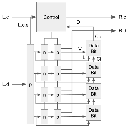
Meanwhile, the datapath shown in Fig. 4 is
somewhat more complex. We use pass transistor logic to reduce its energy
requirements and increase its maximum switching frequency. We use a variant of
the manchester carry chain to check the conditions that are finally fed into
the control block as D. This yields an implementation with high
frequency at low energy and area requirements.
To start, each bit neads to pick between sending Ld or
ext(v) on R in order to implement the bypassing case
with Cs. We do this with pass transistor multiplexers. When
Zd1 is high, it passes the value from Ld to
Rd. When Zd0 is high, it passes the value from
V to Rd. Z is one when the counter is
zero and comes from latching Cn and Cz using the
input acknowledge.
passn(Zd1, Ld0, Rd0)
passp(Zd0, Ld0, Rd0)
passn(Zd0, Vd0, Rd0)
passp(Zd1, Vd0, Rd0)

passn(Zd1, Ld1, Rd1)
passp(Zd0, Ld1, Rd1)
passn(Zd0, Vd1, Rd1)
passp(Zd1, Vd1, Rd1)
Next, we implement the equality checks Dd0 representing Ld=ext(¬v), Dd1 representing Ld=ext(v), and Dd2 representing
!chain(Ld). To do this, each bit will
have two Ci signals and two Co signals.
Cod0 should be low if this and all previous bits are
0, and Cod1 if they are 1. This
effectively forms two parallel carry chains.
passn(Ld0, Cid0, Cod0)
passp(Ld1, Cid0, Cod0)
passn(Ld1, Cid1, Cod1)
passp(Ld0, Cid1, Cod1)
¬Ld0 → Cod0↾
¬Ld1 → Cod1↾
Finally in the MSB, we compare these two carry signals against the carry
chain token value stored in V to implement the equality
checks.
(Cod0 ∨ Vd1) ∧ (Cod1 ∨ Vd0) → Dd0⇂
(Cod0 ∨ Vd0) ∧ (Cod1 ∨ Vd1) → Dd1⇂
¬Cod0 ∧ ¬Vd1 ∨ ¬Cod1 ∧ ¬Vd0 → Dd0↾
¬Cod0 ∧ ¬Vd0 ∨ ¬Cod1 ∧ ¬Vd1 → Dd1↾
¬Dd0 ∧ ¬Dd1 → Dd2↾
Dd0 ∨ Dd1 → Dd2⇂
Compress One
The full compression unit presented above has a few issues when applied to certain problem spaces. First, the total number of bits in the counter dictates the maximum length of any carry chain before incorrect results are given. This means that it doesn't ultimately support arbitrary precision arithmetic. This also means that longer carry chains require logarithmically more counter units making the design area hungry.
Second, it's possible that the carry chain is the full length of the value but the cap token is not part of the carry chain. This implementation would be forced to cut the throughput of such numbers in half by waiting for the whole carry chain to be consumed before emitting it again and moving on. This means that the device can vary drastically between half and full throughput.
Instead of storing and collapsing the whole carry chain, we could impose a limit on the length of the chain and pass the remaining carry chain once that limit is reached. Implementing an arbitrary limit would require an idczfn counter and likely be fairly expensive. However, implementing a limit of one token simply requires a single bit register in the compression unit. This way, we can spread these compression units throughout a computational fabric and execute the compression over the course of multiple operations.
A limit of one also lends itself to an implementation with a guaranteed constant throughput because the stored value is only important when the current input token is the cap. At which point, the stored value is compared against the cap and handled appropriately. Unfortunately, the transition between two input streams complicates the necessary control because there isn't a stored value.
v := 0, n := 0
∗[[ Lc=0 ∧ n=0  →          n := 1, v := Ld; L?
  ▯ Lc=0 ∧ n=1  → R!(v,0);         v := Ld; L?
  ▯ Lc=1 ∧ n=0 ∧ Ld≠v →    n := 1, v := Ld
  ▯ Lc=1 ∧ n=1 ∧ Ld≠v → R!(v,0);   v := Ld
  ▯ Lc=1 ∧ Ld=v → R!(v,1); n := 0, v := Ld; L?
 ]]
So we have to store two values. v records the previous token's
data, and n signals whether v is valid. Luckily,
n is also directly represented by the previous token's control
signifying cap/not cap. We know v isn't yet valid for any token
proceeding a cap token and is valid otherwise.
The first condition handles the first token in the stream. v
isn't valid yet, so we need to load the input data into v and set
n. The second condition handles the majority of the stream.
Lc=0 meaning we haven't reached the end of the stream and
n=1 meaning that we have already seen the first token. In this
case we should forward the previous token stored in v and load the
new input into v.
Then we need to handle the three stream completion cases. In the first case,
the cap token is also the first token of the stream. This case only happens in
the context of a stream representing 0 or -1. To
simplify the circuitry for the output request on R, we load the
input into v and leave the input unacknowledged. This will
transition directly into our last case. In the second case, our stored token is
a different value from the cap token. This means that we cannot compress the
stream. So we forward v and store the new input. Again, we don't
acknowledge the input, transitioning us into our last case. In our last case,
the cap token on the input and the stored value in v are the same,
meaning that we can compress the stream. So, we forward the value in
v as a cap token and acknowledge the input. This completes the
stream and resets n to 0.
Throughout this specification, we've maintained a few constants in an
attempt to optimize the circuitry. First, the data for the output request on
R always comes from v. This removes any muxing from
the datapath and redirects that complexity into the control. Second, the value
stored in v is always set using the data on the input channel
L. These two factors allow us to implement the datapath as a set
of flops that shift the data backwards in the stream by a single pipeline
stage. Third, the control circuitry is only dependent upon an equality test
from the datapath and the datapath is only dependent upon clocking signals from
the control. This allows for a fairly strict separation between the two,
simplifying the control.
There are two primary challenges presented by this spec. The first is that
the clocking signal for the input latches on the input request data
Ld and the clocking signal for the extra set of flops
implementing v are different. v needs to be clocked
on every iteration of the control while the input request should only be
clocked on conditions 1, 2, and 5. The second challenge is that conditions 3
and 4 bypass the delay line on the input request control Lc, but
still change the value of v and therefore of the equality test
between Ld and v. This forces us to create a signal
specifically for those two conditions with its own delay line.
Our implementation starts with the five conditions that drive the output
request on R. Except for Ls, the signals used to
compute these conditions come directly from the spec. Ls is the
extra delay line signal for conditions 3 and 4, and D signals
whether Ld is different from v. Since conditions 3
and 4 can only transition to 4 or 5, only conditions 4 and 5 must check
Ls.
Re ∧      n0 ∧      Ld0 → Rxd0↾
Re ∧      n1 ∧      Ld0 → Rxd1↾
Re ∧      n0 ∧ Dd1 ∧ Ld1 → Rxd2↾
Re ∧ Ls ∧ n1 ∧ Dd1 ∧ Ld1 → Rxd3↾
Re ∧ Ls ∧      Dd0 ∧ Ld1 → Rxd4↾
Then, we use these conditions to drive the output request, the input enable, and the extra delay signal. Because conditions 1 and 3 only serve to load the input into the internal memory, they don't forward any request on the output. Furthermore, conditions 3 and 4 redirect the control to condition 5 and therefore don't acknowledge the input request.
¬_Rxd1 ∨ ¬_Rxd3 → Rd0↾
Rd1 = Rxd4

Rxd0 ∨ Rxd1 ∨ Rxd4 → Le⇂
Rxd2 ∨ Rxd3 → Ls⇂
Because the value of the input control token is reflected in the output
request rails, we can use them to set the internal memory unit for
n. Conditions 1 and 3 set n to 1 while
condition 5 sets it to 0. The value of n for
conditions 2 and 4 is already set correctly. We then use the output request
reset to acknowledge the transitions on the internal memory and reset the input
acknowledges. The delay line for Ls is placed between the driver
and all proceeding usages.
(¬n0 ∨ ¬Ld0 ∧ ¬_Rxd0 ∨  ¬Ls ∧ ¬_Rxd2) → n1↾
  n0 ∧ (Ld0 ∨  _Rxd0) ∧ (Ls ∨  _Rxd2) → n1⇂
 ¬n1 ∨ ¬Re ∧  ¬_Rxd4  → n0↾
  n1 ∧ (Re ∨   _Rxd4) → n0⇂

       ¬Ld0 ∧ ¬n0 → Rxd0⇂
¬Re ∧ ¬Ld0       → Rxd1⇂
      ¬Ls ∧ ¬n0 → Rxd2⇂
¬Re ∧ ¬Ls       → Rxd3⇂
¬Re ∧ ¬Ld1 ∧ ¬n1 → Rxd4⇂

_Rxd1 ∧ _Rxd3 → Rd0⇂

¬Rxd0 ∧ ¬Rxd1 ∧ ¬Rxd4 → Le↾
¬Rxd2 ∧ ¬Rxd3 → Ls↾
To implement the datapath in Fig. 5, the first thing
we have to do is generate the clocking signal for v using
Le and Ls. Meanwhile, the clock signal for the
input data is just Le.
Ls ∧ Le → vclk↾
¬Ls ∨ ¬Le → vclk⇂
Then, we need to implement the equality check between Ld and
v for each bit.
Ld0 ∧ Rd1 ∨ Ld1 ∧ Rd0 → Cd0⇂
¬Ld0 ∧ ¬Rd0 ∨ ¬Ld1 ∧ ¬Rd1 → Cd0↾
Cd0 → Cd1⇂
¬Cd0 → Cd1↾
We take inspiration from a Manchester Carry Chain to propagate this equality check across the bits using pass transistors.
passn(Cd0, Di, Do)
passp(Cd1, Di, Do)
¬Cd0 → Do↾
And finally, we generate the one hot encoding D for the
equality check used in the control.
Dd1 = Do
Do → Dd0⇂
¬Do → Dd0↾
Evaluation
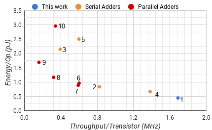
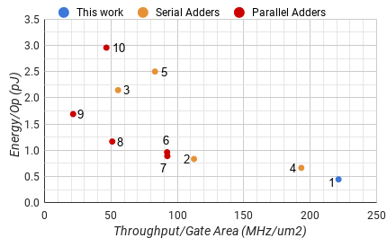
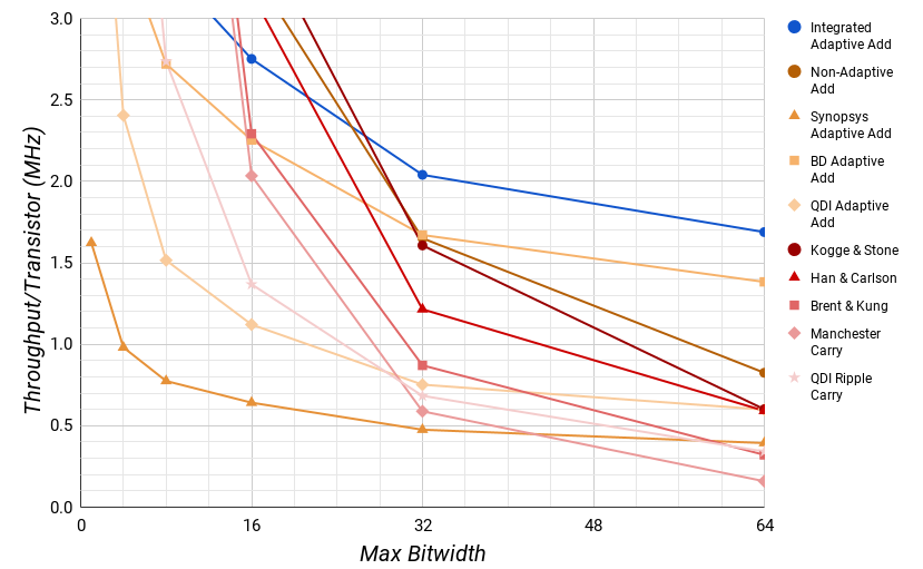
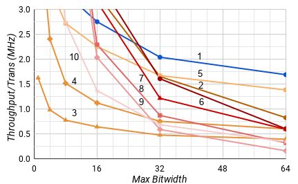
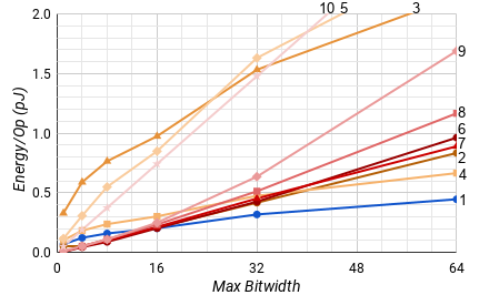
Aside from the Integrated Adaptive adder found in this paper (1), we developed other serial adders for comparison including a clocked non-adaptive digit-serial adder (2), a clocked adaptive digit-serial adder synthesized by Synopsys Design Compiler (3), a BD adaptive serial adder (4), and a QDI adaptive serial adder (5). Furthermore, we built a set of parallel adders including clocked Kogge & Stone[20] (6), Han & Carlson[22] (7), and Brent & Kung[21] (8) carry lookahead adders, a clocked Manchester Carry Chain[23] (9), and a QDI ripple carry adder[24] (10). Each adder is labelled on graphs by their associated number.
We used a set of in-house tools to develop and evaluate all of these circuits. We verify the production rule specifications with a switch-level simulation which identifies instability, interference, and deadlock. We then automatically translate these specifications into netlists and verify their analog properties using Synopsys's combined simulator with VCS, a verilog simulator, to simulate the testbench and HSIM, a fast spice simulator, to report power and performance metrics. We simulated the CHP using C++ to generate inject and expect values which we tied into both the switch level and analog simulations using Python. This allowed us to verify circuit and behavioral correctness by checking the behavioral, digital, and analog simulations against each other.
We used Intel PIN to analyze the Spec2006 integer bitwidth distribution presented in Fig. 1. Ultimately, it is measured across 2 trillion integer add instructions executed by the 29 applications listed below selected by the Spec Benchmark Committee to be a measure of a realistic workload [7][8]. (perlbench, bwaves, milc, cactusADM, gobmk, povray, sjeng, h264ref, omnetpp, sphinx3, bzip2, gamess, zeusmp, leslie3d, dealII, calculix, GemsFDTD, tonto, astar, xalancbmk, gcc, mcf, gromacs, namd, soplex, hmmer, libquantum, lbm, wrf) The bitwidths are measured from the max of all of the inputs for each add instruction. Video compression from h264ref and audio processing from sphinx3 each exhibited better bitwidth distributions than the one shown in Fig. 1 with an average bitwidth of 6.7 and 10.9 bits respectively, not including the spike for memory address calculations. (8.7 and 11.5 bits including the spike)
To evaluate the energy per operation and throughput of these circuits, we
used a 1V 28nm process to simulate uniform random inputs for the serial adders
and 1, 4, 8, 16, 32, and 64 bit versions of the parallel adders. We then
compare their performance in the context of Spec2006's integer bitwidth
distribution as shown in Fig. 1 ignoring the
spike at 48 bits since memory address calculations should be done by a
bit-parallel datapath. To get more accurate results, we protected each of the
digitally driven channels with a FIFO of three WCHB buffers, and the clock
signal with 6 six inverters, all isolated to a separate testbench power source.
We hand-sized all of the adders to optimize delay. However, this mostly
came out to minimal gate sizing with a pn-ratio of 2.
We count the transistors in each design from the generated spice file and
also computed the sum of all the gate areas for each design as estimates for
layout area. While we found the transistor count metric more approachable, the
trends remain the same across both metrics. In all of our
implementations, we avoid using the Half Cycle Timing Assumption (HCTA) [17] when possible and use weak feedback for C-elements.
Circuitry necessary for reset was not included in any the above
descriptions.
Fig. 6 shows the average addition throughput per transistor versus the energy per add of each adder. For a 4-bit datapath, our serial adder requires 314 transistors with a total gate area of 2.395 um2. This is fewer than the 330 transistors with a total gate area of 2.479 um2 necessary for the clocked non-adaptive serial adder because our design is only half-buffered, latching each input with 14 transistors each instead of using standard master-slave D flip-flops with 28 each. This reduces the latching overhead from 252 transistors to 112. And while our design operates at half the frequency using slightly more energy per token, this overhead allows our adder to skip a majority of the tokens whereas the non-adaptive design cannot. This translates to a 1.9 times increase in throughput from 279 MHz to an average of 530.3 MHz, and a 46.5% decrease in energy from 833 fJ to an average of 445 fJ.
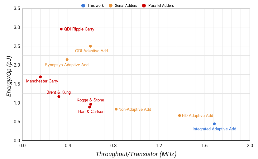
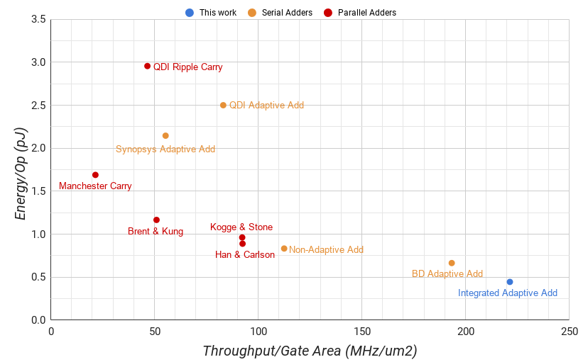
The most competitive 64 bit parallel adder, the Han & Carlson, has 6552 transistors with a total gate area of 41.92 um2. Its operation throughput is 7.31 times ours at 3.878 GHz. However, if we were to devote the same transistor count to multiple instances of our adder, they would have an average of 11 GHz, using 50% less energy per operation.
The synchronous adaptive adder synthesized by Synopsys uses twice as many transistors at 616 and has 54% lower operation throughput at 242 MHz. Furthermore, it uses 4.8 times the energy per operation. This difference is likely because the design is synthesized using a standard cell library while the rest are full custom.
Adaptivity requires stateful control-flow either in the form of a val-rdy interface or some asynchronous channel protocol. The devices best geared to implement stateful control flow are asymmetric c-elements. These don't really exist in any standard-cell libraries because of the gross number of possible cells. For this reason, good self-timed circuits often custom-layout these cells for each design. Synthesizers don't have this option though. Instead they cobble together stateful control from latches, flops, and combinational logic which is ultimately not a good fit.
In the datapath, our adder uses latches on the data while the synthesizer used flops, dramatically increasing the transistor count. Furthermore, our adder used a 4-bit Manchester Carry Chain while the synthesized implementation uses full-adder cells from the standard-cell library, ultimately implementing a normal Ripple Carry Adder. This means that while our adder can operate at 1.85 GHz, the synthesized adder is limited to 1 GHz.
All of these differences are fairly typical in synthesized vs full-custom and the synthesis could be tuned to produce a better result. In recognition of this we also set out to design a full custom latched synchronous adaptive adder. In the end, it required a val-rdy interface because the input streams are variable-length. The circuitry required to implement a val-rdy interface is ultimately near-identical to the circuitry required to implement a bundled-data interface. The only difference is that for the val-rdy interface, the control signals are clocked instead of delayed with a delay line. So, this design ended up being the BD Adaptive Add (4). Ultimately, the architecture is very similar to our integrated design. At 358 transistors, it burns only 1.5 times the energy per operation with only 4.5% lower operation throughput.
The only adaptive self-timed adder in the literature is from Bitsnap [35]. We did not compare against this adder because the implementation of its adaptivity was not self contained. The design of the adder is ultimately a single bit from the ripple-carry adder labelled (10) with its carry-out fed back into the carry in through a FIFO. The implementation of the control relied heavily upon the Bitsnap Microprocessor architecture as a whole and was entirely inseparable. The QDI self-timed adaptive adder labelled (5) that we developed is the self-contained version of this. It is ultimately more expensive than other approaches due to acknowledgement requirements between the control and the datapath, implementing a 1 bit datapath with 423 transistors, 44% lower operation throughput, and burning 5.4 times as much energy per operation.
Fig. 8 compares the throughput per transistor efficiency for a single add against custom hardware for a given bitwidth. For a single 32 bit or wider operation the Integrated Adaptive adder has a similar throughput per transistor efficiency to a custom bitwidth Brent & Kung carry lookahead adder. Below 32 bits, the dedicated custom bitwidth parallel adders have significantly better throughput per transistor efficiency. This is largely due to the requirement that the cap token be all ones or all zeros.
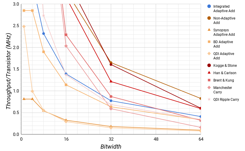
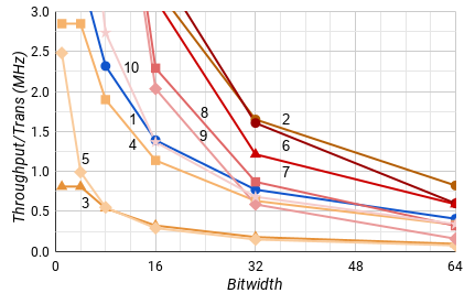
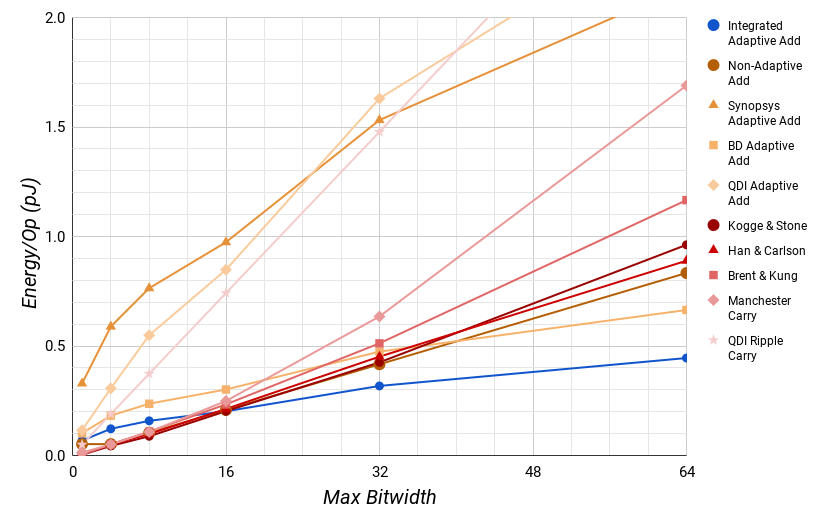
However, most computational systems don't have hardware specifically dedicated to every bitwidth. Fig. 9 shows the performance of these adders on average for a given maximum bitwidth using the bitwidth distribution from Spec2006. At 26 bits, the Integrated Adaptive adder has the same average throughput efficiency as the Kogge & Stone adder. Once above 26 bits, the average throughput efficiency of the Integrated Adaptive adder is significantly better than any other architecture.
The story for the energy per operation metric is fairly similar in Fig. 10. For a single operation, the custom width parallel adders use about 40% less energy across the board.
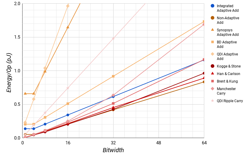
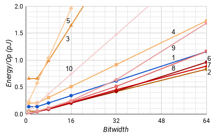
However, when we look at the average behavior for a maximum bitwidth in Fig. 11, this lead only exists below 16 bits. For widths of more than 16, the Integrated Adaptive adder uses significantly less energy on average.
The compression units are much more difficult to evaluate overall. For the compress1 units, we know that they always delay the stream by one token, but then retain full throughput for the rest of the stream. The QDI compress1 unit with 166 transistors has the highest frequency and lowest energy per token at 2.21 GHz and 37.7 fJ. However, it only has one bit per token while the BD and integrated implementations have 4. The BD compress1 unit with 368 transistors has the lowest frequency and highest energy per token at 1.43 GHz and 121.6 fJ. However, the integrated implementation with 433 transistors is once again the most performant, with a frequency and energy of 2.20 GHz and 82.5 fJ per token.
For the full compression units, there are three modes. The first mode passes tokens that aren't all ones or all zeroes and therefore aren't part of any carry chain. The second mode stores up a carry chain into the counter, and the third drains it from the counter. Tokens in a carry chain must always go through both the second and third modes meaning the overall frequency is halved. For the QDI implementation, this encompasses every token because tokens are only one bit and therefore always all ones or all zeros. This means that the QDI implementation has no passing mode. The wider the pipeline, the more likely the token will have at least one bit that is different making the token passable. This means that the BD and integrated implementations ultimately won't encounter modes 2 and 3 very often. However, we do have to measure the cycle frequency of the unit instead of the input or output frequency.
Not including the counter, the QDI compressN unit has 166 transistors, a frequency of 2.6 GHz and energy of 43 fJ per token. The BD compressN unit has 368 transistors, operating at 1.7 GHz and using 101.6 fJ per token. The integrated compressN strikes the best of both with 334 transistors operating at 2.0 GHz and using 75 fJ per token.
With respect to the adder, this is a fairly large overhead. However, these units ultimately should not be used very often. In general it is more performant to just accept the overhead of extra tokens instead of trying to compress them within the execution logic. Streams should ultimately be compressed only when they are being read from memory. With four bit tokens, input streams will be an average of 3 tokens long. While an overflow event or a bitwise operator can make every token in a stream redundant, that ultimately means 3 tokens in a redundant stream versus 1 token in a compressed one.
Conclusion
The digit-serial adaptive adder presented in this paper has significantly higher throughput for the same number of transistors at a much lower energy cost than every other industry standard and many other non-standard approaches.
Going forward, this adder represents only one of the many operators required for a fully functional computational system. We will explore other digit serial operators and their behavior in larger contexts, modifying the control presented in this paper to create a full featured LSB first digit-serial ALU. We will also apply the lessons learned in this paper toward the exploration of MSB first arithmetic, and its use in larger contexts.
Appendix
CHP Notation
Communicating Hardware Processes (CHP) is a hardware description language used to describe clockless circuits derived from C.A.R. Hoare's Communicating Sequential Processes (CSP) [1]. A full description of CHP and its semantics can be found in [2]. Below is an informal description of that notation listed top to bottom in descending precedence.
- Skip
skipdoes nothing and continues to the next command. - Dataless Assignment
c↾sets the voltage of the nodectoVddandc⇂sets it toGND. - Assignment
a := ewaits until the expression, e, has a valid value, then assigns that value to the variable,a. - Send
X!ewaits until the expressionehas a valid value, then sends that value across the channelX.X!is a dataless send. - Receive
X?awaits until there is a valid value on the channelX, then assigns that value to the variablea.X?is a dataless receive. - Probe
Xreturns the value to be received from the channelXwithout executing a receive. - Sequential Composition
S; Texecutes the programsSfollowed byT. - Parallel Composition
S ∥ Texecutes the programsSandTin any order. - Deterministic Selection
[G1 → S1▯…▯Gn → Sn]whereGiis a guard andSiis a program. A guard is a dataless expression or an expression that is implicitly cast to dataless. This waits until one of the guards,Gi, evaluates toVdd, then executes the corresponding program,Si. The guards must be mutually exclusive. The notation[G]is shorthand for[G → skip]. - Repetition
∗[G1 → S1▯…▯Gn → Sn]is similar to the selection statements. However, the action is repeated until no guard evaluates toVdd.∗[S]is shorthand for∗[true → S].
PRS Notation
In a Production Rule Set (PRS), a Production Rule is a compact way to
specify a single pull-up or pull-down network in a circuit. An alias
a = b aliases two names to one circuit node. A rule G
→ A represents a guarded action where G is a guard (as
described above) and A is a dataless assignment as described
above. A gate is made up of multiple rules that describe the up and down
assignments. The guard of each rule in a gate represents a part of the pull-up
or pull-down network of that gate depending upon the corresponding assignment.
If the rules of a gate do not cover all conditions, then the gate is
state-holding with a staticizer. For such a gate driving a node X,
the internal node before the staticizor is referenced as _X.
Finally, a pass transistor is specified with passn(gate, source,
drain) or passp(gate, source, drain).
References
Communicating Sequential Processes. Communications of the ACM, pages 666-677, 1978.
Synthesis of Asynchronous VLSI Circuits. Computer Science Department at California Institute of Technology: Caltech-CS-TR-93-28, 1991.
Principles Asynchronous Circuit Design.Kluwer Academic Publishers, 2002.
QDI Constant Time Counters. IEEE Transactions on VLSI.
Dynamic effective precision matching computation.Proc. of 11th Workshop on Synthesis and System Integration of Mixed Information Technologies SASIMI, Hiroshima. 2003.
Dynamically exploiting narrow width operands to improve processor power and performance.High-Performance Computer Architecture, 1999. Proceedings. Fifth International Symposium On. IEEE, 1999.
SPEC CPU2000.2000.
SPEC CPU2006.2006.
Parallel Computer Architecture: A Hardware/Software Approach.Gulf Professional Publishing, 1999, pg 15-16.
Quantitative analysis of culture using millions of digitized books.Science. 2011.
CPU DB: recording microprocessor history.Queue 10.4 (2012): 10.
The Design of an Asynchronous MIPS R3000 Microprocessor.ARVLSI. Vol. 97. 1997.
Computer Arithmetic: Principles, Architectures, and VLSI Design.Personal publication, (1999).
Binary Adder Architectures for Cell-Based VLSI and their Synthesis.Hartung-Gorre, 1998.
Optimization of the Binary Adder Architectures Implemented in ASICs and FPGAs.Soft Computing Applications (2013): 295-308.
An Evaluation of Asynchronous Addition.IEEE Transactions on Very Large Scale Integration (VLSI) Systems 4.1 (1996): 137-140.
Reducing power consumption with relaxed quasi delay-insensitive circuits.Asynchronous Circuits and Systems, 2009. ASYNC'09. 15th IEEE Symposium on. IEEE, 2009.
A taxonomy of parallel prefix networks.Signals, Systems and Computers, 2004. Conference Record of the Thirty-Seventh Asilomar Conference on. Vol. 2. IEEE, 2003.
Simultaneous Carry Adder.US Patent 2,966,305, December 27, 1957.
A Parallel Algorithm for the Efficient Solution of a General Class of Recurrence Equations.IEEE Transactions on Computers, 1973, C-22, 783-791
A regular layout for parallel adders.IEEE transactions on Computers 3 (1982): 260-264.
Fast area-efficient VLSI adders.Computer Arithmetic (ARITH), 1987 IEEE 8th Symposium on. IEEE, 1987.
Parallel Addition in Digital Computers: A New Fast 'Carry' Circuit.Proceedings of the IEE-Part B: Electronic and Communication Engineering 106.29 (1959): 464-466.
Pipelined asynchronous circuits.(1998).
High Speed Binary Adder.IBM J. Reasearch. Dev., Vol. 25, No. 3, p.156, May, 1981.
A Sub-Nanosecond 0.5um 64b Adder Design.IEEE International Solid-State Circuits Conference 1996.
Energy-Delay Characteristics of CMOS Adders. High-Performance Energy-Efficient Microprocessor Design. Series on Integrated Circuits and Systems. p. 147.
Bit-Serial Inner Product Processors in VLSI.(1981): 155-164.
Serial-Data Computation.Vol. 39. Springer Science & Business Media, 2012.
Digit-Serial Computation.pp 6, 15, and 25, Springer Science & Business Media, 2012.
Digital Arithmetic.Elsevier, 2004.
High-Performance Bit-Serial Datapath Implementation for Large-Scale Configurable Systems.Penn State University, pp 33, April 1996.
Asynchronous Logic in Bit-Serial Arithmetic.IEEE International Conference on Electronics, Circuits and Systems, pp. 175-178, September 1998.
The Connection Machine: A Computer Architecture Based on Cellular Automata.Physica D: Nonlinear Phenomena 10.1 (1984): 213-228.
Bitsnap: Dynamic Significance Compression for a Low-energy Sensor Network Asynchronous Processor.Asynchronous Circuits and Systems, 2005. ASYNC 2005. Proceedings. 11th IEEE International Symposium on. IEEE, 2005.
A novel digit-serial systolic array for modular multiplication.Circuits and Systems, 1998. ISCAS'98. Proceedings of the 1998 IEEE International Symposium on. Vol. 2. IEEE, 1998.
Bit-level pipelined digit-serial array processors.IEEE Transactions on Circuits and Systems II: Analog and Digital Signal Processing 45.7 (1998): 857-868.
Very low power pipelines using significance compression.Proceedings of the 33rd annual ACM/IEEE international symposium on Microarchitecture. ACM, 2000.
 Ned Bingham is a PhD student at Yale. He received his B.S. (2013) and
M.S. (2017) from Cornell. During his Masters, he designed a set of tools for
working with self-timed systems using a control-flow specification called
Handshaking Expansions. Currently, he is researching self-timed systems as a
method of leveraging average workload characteristics in general compute
architectures. Between his studies, he has worked at Intel on Pre-Silicon
Validation (2011, 2012), Qualcomm researching arithmetic architecture (2014),
and Google researching self-timed systems (2016). In his spare time, he reads
about governmental systems and dabbles in building collaborative tools. (www.nedbingham.com)
Ned Bingham is a PhD student at Yale. He received his B.S. (2013) and
M.S. (2017) from Cornell. During his Masters, he designed a set of tools for
working with self-timed systems using a control-flow specification called
Handshaking Expansions. Currently, he is researching self-timed systems as a
method of leveraging average workload characteristics in general compute
architectures. Between his studies, he has worked at Intel on Pre-Silicon
Validation (2011, 2012), Qualcomm researching arithmetic architecture (2014),
and Google researching self-timed systems (2016). In his spare time, he reads
about governmental systems and dabbles in building collaborative tools. (www.nedbingham.com)
 Rajit Manohar is the John C. Malone Professor of Electrical
Engineering and Professor of Computer Science at Yale. He received his B.S.
(1994), M.S. (1995), and Ph.D. (1998) from Caltech. He has been on the Yale
faculty since 2017, where his group conducts research on the design, analysis,
and implementation of self-timed systems. He is the recipient of an NSF CAREER
award, nine best paper awards, nine teaching awards, and was named to MIT
technology review's top 35 young innovators under 35 for contributions to low
power microprocessor design. His work includes the design and implementation
of a number of self-timed VLSI chips including the first high-performance
asynchronous microprocessor, the first microprocessor for sensor networks, the
first asynchronous dataflow FPGA, the first radiation hardened SRAM-based FPGA,
and the first deterministic large-scale neuromorphic architecture. Prior to
Yale, he was Professor of Electrical and Computer Engineering and a Stephen H.
Weiss Presidential Fellow at Cornell. He has served as the Associate Dean for
Research and Graduate studies at Cornell Engineering, the Associate Dean for
Academic Affairs at Cornell Tech, and the Associate Dean for Research at
Cornell Tech. He founded Achronix Semiconductor to commercialize
high-performance asynchronous FPGAs. (csl.yale.edu/~rajit)
Rajit Manohar is the John C. Malone Professor of Electrical
Engineering and Professor of Computer Science at Yale. He received his B.S.
(1994), M.S. (1995), and Ph.D. (1998) from Caltech. He has been on the Yale
faculty since 2017, where his group conducts research on the design, analysis,
and implementation of self-timed systems. He is the recipient of an NSF CAREER
award, nine best paper awards, nine teaching awards, and was named to MIT
technology review's top 35 young innovators under 35 for contributions to low
power microprocessor design. His work includes the design and implementation
of a number of self-timed VLSI chips including the first high-performance
asynchronous microprocessor, the first microprocessor for sensor networks, the
first asynchronous dataflow FPGA, the first radiation hardened SRAM-based FPGA,
and the first deterministic large-scale neuromorphic architecture. Prior to
Yale, he was Professor of Electrical and Computer Engineering and a Stephen H.
Weiss Presidential Fellow at Cornell. He has served as the Associate Dean for
Research and Graduate studies at Cornell Engineering, the Associate Dean for
Academic Affairs at Cornell Tech, and the Associate Dean for Research at
Cornell Tech. He founded Achronix Semiconductor to commercialize
high-performance asynchronous FPGAs. (csl.yale.edu/~rajit)